| dc.contributor.advisor | Santos, Michael B | |
| dc.creator | Gaspe, Chomani Kishanika | |
| dc.date.accessioned | 2019-04-27T21:28:15Z | |
| dc.date.available | 2019-04-27T21:28:15Z | |
| dc.date.issued | 2013 | |
| dc.identifier | 99215824902042 | |
| dc.identifier.uri | https://hdl.handle.net/11244/318770 | |
| dc.description.abstract | In this work the electronic properties of n-type and p-type quantum wells (QWs) made of narrow gap InSb and InGaAs materials have been studied experimentally. The narrower band gap in these materials leads to smaller effective masses for electrons and holes, therefore higher mobilities are expected. High intrinsic electron mobility due to the small effective mass for electrons in these materials makes them attractive as the channel material in n-type transistors. The layer structure, doping and growth parameters were further optimized to enhance the mobility for electrons in InSb and InGaAs QWs. A room-temperature electron mobility of 11,600cm2/Vs and 44,700cm2/Vs were achieved in our QWs made of In0.64Ga0.36As and InSb, respectively. | |
| dc.description.abstract | The hole effective mass in InSb QWs with different strain and confinement was studied. To achieve high hole mobilities, strain and confinement must be maximized. Both parameters increase the energy splitting between heavy and light hole bands and lower the effective mass for in-plane motion. The smallest hole effective mass of 0.017me was observed in an InSb QW with 1.05% strain and 7nm well width. Hole mobility in strained InSb QWs grown on GaAs(001) substrates can be significantly improved by better buffer layer design. The effect of the thickness and the Al composition in the Alxln1-xSb initial buffer layer on hole mobility of p-type InSb QWs was also studied. A room-temperature hole mobility of 1,050cm2/Vs has been achieved in our improved p-type InSb QW with 1.32% strain, 7nm well width and a 0.8μm thick Al0.15In0.85Sb initial buffer layer. The compressive strain was introduced into InyGa1-yAs QWs by increasing the Indium composition (y) in the well slightly above the value needed for lattice matching (y=0.53) with InP (001) substrates. A room temperature hole mobility of 230cm2/Vs was obtained in our In0.75Ga0.25As QW with remotely, Be delta-doped In0.45Al0.55As barrier layers. | |
| dc.description.abstract | An experimental study of growth, structural and electronic properties of elemental Sb QWs with GaSb barriers was performed to explore their potential as topological insulators. Molecular beam epitaxy growth procedures on GaAs(111)A and GaSb(111)A were developed to realize ultra-thin layers of Sb with a thickness ≤ 4nm. Transmission electron microscopy and scanning electron microscopy indicated good crystalline quality in these ultra-thin layers of Sb. Resistivity measurements indicated that Sb QWs with a thickness above ~2nm were metallic, whereas thinner wells showed insulating behavior. | |
| dc.format.extent | 171 pages | |
| dc.format.medium | application.pdf | |
| dc.language | en_US | |
| dc.relation.requires | Adobe Acrobat Reader | |
| dc.subject | Molecular beam epitaxy | |
| dc.subject | Quantum wells | |
| dc.subject | Electron transport | |
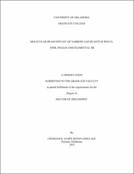
| dc.title | Molecular Beam Epitaxy of Narrow Gap Quantum Wells: InSb, InGaAs and Elemental Sb | |
| dc.type | text | |
| dc.type | document | |
| dc.thesis.degree | Ph.D. | |
| ou.group | College of Arts and Sciences::Homer L. Dodge Department of Physics and Astronomy | |
