| dc.date.accessioned | 2015-07-23T15:35:23Z | |
| dc.date.available | 2015-07-23T15:35:23Z | |
| dc.date.issued | 1982-09-07 | |
| dc.identifier | pat4348428 | |
| dc.identifier.uri | https://hdl.handle.net/11244/15327 | |
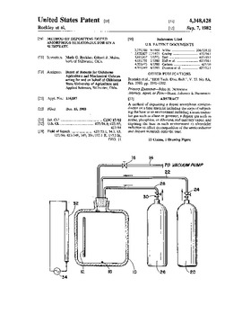
| dc.description.abstract | A method of depositing a doped amorphous semiconductor on a base material including the steps of subjecting the base to an environment including a semiconductor gas such as silane or germane, a dopant gas such as arsine, phosphine, or diborane, and mercury vapor, and exposing the base in such environment to ultraviolet radiation to effect decomposition of the semiconductor and dopant materials onto the base. | |
| dc.format | application/pdf | |
| dc.format.extent | 4 pages | |
| dc.language | en_US | |
| dc.publisher | U.S. Patent and Trademark Office | |
| dc.title | Method of Depositing Doped Amorphous Semiconductor on a Substrate | |
| dc.type | text | |
| osu.filename | pat4348428.pdf | |
| osu.accesstype | Open Access | |
| dc.type.genre | Patent | |
| dc.contributor.inventor | Rockley, Mark G. | |
| dc.contributor.inventor | Mains, Gilbert J. | |
| dc.identifier.patentID | 4,348,428 | |
| dc.date.filed | 1980-12-15 | |
| dc.contributor.assignee | Board of Regents/Oklahoma State University and the A & M Colleges | |
| dc.subject.primaryusclass | 438/482 | |
| dc.subject.otherusclasses | 136/258 | |
| dc.subject.otherusclasses | 257/E21.101 | |
| dc.subject.otherusclasses | 427/585 | |
| dc.subject.otherusclasses | 438/903 | |
| dc.subject.otherusclasses | 438/96 | |
| dc.subject.cpcclasses | C23C 16/482 (20130101) | |
| dc.subject.cpcclasses | H01L 21/0262 (20130101) | |
| dc.subject.cpcclasses | H01L 21/02576 (20130101) | |
| dc.subject.cpcclasses | H01L 21/02532 (20130101) | |
| dc.subject.cpcclasses | Y10S 438/903 (20130101) | |