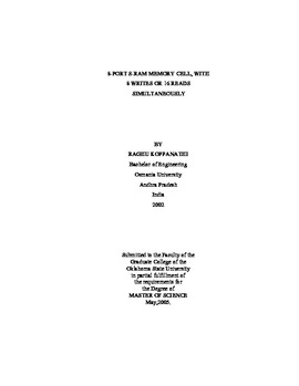
| dc.contributor.advisor | Johnson, Louis G. | |
| dc.contributor.author | Koppanathi, Raghu | |
| dc.date.accessioned | 2014-04-17T20:08:49Z | |
| dc.date.available | 2014-04-17T20:08:49Z | |
| dc.date.issued | 2005-05-01 | |
| dc.identifier.uri | https://hdl.handle.net/11244/10230 | |
| dc.description.abstract | The main purpose of this thesis is to understand the working principle and design of an 8-port SRAM Memory cell with an emphasis to attain maximum possible Noise margin. We have proposed four designs, namely 2-SRAM, 4-SRAM, 8-SRAM, and J-SRAM capable of 8 writes or 16 reads simultaneously. Worst case scenarios in reading from and writing into a memory cell are considered and analyzed. Theoretical analysis is done using a simplified BSIM3v3 model, equations derived for inverter threshold voltage, node and complementary nodes on the memory cell are used to calculate static noise margin of the cell. Layout designs of the models are made in Cadence Virtuoso Layout Editor, and simulations are run for measuring dynamic noise margin in the cell using Cadence Spectre simulator. Designs are made with transistor widths giving maximum noise margin that is possible in with a limited area of 1600 �m2. The simulated results and the theoretical results are then compared.Results and Conclusions: The performances of the four designs are compared with respect to noise margin. With read access time (5ns) and silicon area the same for all the designs, noise margin is measured, and it is found that J-SRAM has the maximum noise margin of 0.8251 V for a 5 V supply in an AMI 0.6� technology. This design is also tested for read access time of 1.5ns, and the noise margin obtained is above 0.5V. If the limitation on silicon area is neglected, then a noise margin of 2V is obtained. | |
| dc.format | application/pdf | |
| dc.language | en_US | |
| dc.publisher | Oklahoma State University | |
| dc.rights | Copyright is held by the author who has granted the Oklahoma State University Library the non-exclusive right to share this material in its institutional repository. Contact Digital Library Services at lib-dls@okstate.edu or 405-744-9161 for the permission policy on the use, reproduction or distribution of this material. | |
| dc.title | 8-Port SRAM Memory Cell, with 8 Writes or 16 Reads Simultaneously | |
| dc.type | text | |
| dc.contributor.committeeMember | Zhang, Yumin | |
| dc.contributor.committeeMember | Ramakumar, R.G. | |
| osu.filename | Koppanathi_okstate_0664M_1359.pdf | |
| osu.college | Engineering, Architecture, and Technology | |
| osu.accesstype | Open Access | |
| dc.description.department | School of Electrical & Computer Engineering | |
| dc.type.genre | Thesis | |
